- 您现在的位置:买卖IC网 > Sheet目录3831 > PIC18F2515-I/SO (Microchip Technology)IC MCU FLASH 24KX16 28SOIC
PIC18F2X1X/4X1X
DS39636D-page 146
2009 Microchip Technology Inc.
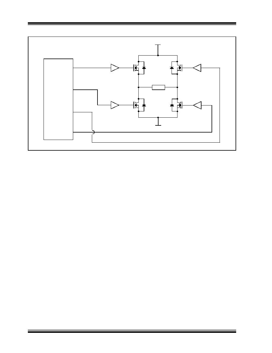
FIGURE 15-7:
EXAMPLE OF FULL-BRIDGE APPLICATION
15.4.5.1
Direction Change in Full-Bridge Mode
In the Full-Bridge Output mode, the P1M1 bit in the
CCP1CON register allows user to control the forward/
reverse direction. When the application firmware
changes this direction control bit, the module will
assume the new direction on the next PWM cycle.
Just before the end of the current PWM period, the
modulated outputs (P1B and P1D) are placed in their
inactive state, while the unmodulated outputs (P1A and
P1C) are switched to drive in the opposite direction.
This occurs in a time interval of 4 TOSC * (Timer2
Prescale Value) before the next PWM period begins.
The Timer2 prescaler will be either 1, 4 or 16, depend-
ing on the value of the T2CKPS bit (T2CON<1:0>).
During the interval from the switch of the unmodulated
outputs to the beginning of the next period, the
modulated outputs (P1B and P1D) remain inactive.
This relationship is shown in Figure 15-8.
Note that in the Full-Bridge Output mode, the CCP1
module does not provide any dead-band delay. In
general, since only one output is modulated at all times,
dead-band delay is not required. However, there is a
situation where a dead-band delay might be required.
This situation occurs when both of the following
conditions are true:
1.
The direction of the PWM output changes when
the duty cycle of the output is at or near 100%.
2.
The turn-off time of the power switch, including
the power device and driver circuit, is greater
than the turn-on time.
Figure 15-9 shows an example where the PWM
direction changes from forward to reverse at a near
100% duty cycle. At time t1, the outputs P1A and P1D
become inactive, while output P1C becomes active. In
this example, since the turn-off time of the power
devices is longer than the turn-on time, a shoot-through
current may flow through power devices, QC and QD
(see Figure 15-7), for the duration of ‘t’. The same
phenomenon will occur to power devices, QA and QB,
for PWM direction change from reverse to forward.
If changing PWM direction at high duty cycle is required
for an application, one of the following requirements
must be met:
1.
Reduce PWM for a PWM period before
changing directions.
2.
Use switch drivers that can drive the switches off
faster than they can drive them on.
Other options to prevent shoot-through current may
exist.
P1A
P1C
FET
Driver
FET
Driver
V+
V-
Load
FET
Driver
FET
Driver
P1B
P1D
QA
QB
QD
QC
PIC18F4X1X
发布紧急采购,3分钟左右您将得到回复。
相关PDF资料
DSPIC33FJ128GP202-I/SP
IC DSPIC MCU/DSP 128K 28DIP
PIC24FJ128GA310-I/BG
MCU 16BIT 128KB FLASH 121TFBGA
PIC24HJ128GP204-I/PT
IC PIC MCU FLASH 128K 44TQFP
PIC18F8393-I/PT
IC PIC MCU FLASH 4KX16 80TQFP
DSPIC33FJ128GP204-I/PT
IC DSPIC MCU/DSP 128K 44TQFP
DSPIC33FJ64MC802-I/MM
IC DSPIC MCU/DSP 64K 28-QFN
PIC16F876A-I/SS
IC MCU FLASH 8KX14 EE 28SSOP
PIC24HJ128GP202-I/SP
IC PIC MCU FLASH 128K 28DIP
相关代理商/技术参数
PIC18F2515-I/SP
功能描述:8位微控制器 -MCU 48KB 3968 RAM 25 I/O RoHS:否 制造商:Silicon Labs 核心:8051 处理器系列:C8051F39x 数据总线宽度:8 bit 最大时钟频率:50 MHz 程序存储器大小:16 KB 数据 RAM 大小:1 KB 片上 ADC:Yes 工作电源电压:1.8 V to 3.6 V 工作温度范围:- 40 C to + 105 C 封装 / 箱体:QFN-20 安装风格:SMD/SMT
PIC18F2515T-I/SO
功能描述:8位微控制器 -MCU 48KB 3968 RAM 25 I/O RoHS:否 制造商:Silicon Labs 核心:8051 处理器系列:C8051F39x 数据总线宽度:8 bit 最大时钟频率:50 MHz 程序存储器大小:16 KB 数据 RAM 大小:1 KB 片上 ADC:Yes 工作电源电压:1.8 V to 3.6 V 工作温度范围:- 40 C to + 105 C 封装 / 箱体:QFN-20 安装风格:SMD/SMT
PIC18F2520-E/ML
功能描述:8位微控制器 -MCU 32KB 3968 RAM 25I/O RoHS:否 制造商:Silicon Labs 核心:8051 处理器系列:C8051F39x 数据总线宽度:8 bit 最大时钟频率:50 MHz 程序存储器大小:16 KB 数据 RAM 大小:1 KB 片上 ADC:Yes 工作电源电压:1.8 V to 3.6 V 工作温度范围:- 40 C to + 105 C 封装 / 箱体:QFN-20 安装风格:SMD/SMT
PIC18F2520-E/SO
功能描述:8位微控制器 -MCU 32KB 3968 RAM 25I/O RoHS:否 制造商:Silicon Labs 核心:8051 处理器系列:C8051F39x 数据总线宽度:8 bit 最大时钟频率:50 MHz 程序存储器大小:16 KB 数据 RAM 大小:1 KB 片上 ADC:Yes 工作电源电压:1.8 V to 3.6 V 工作温度范围:- 40 C to + 105 C 封装 / 箱体:QFN-20 安装风格:SMD/SMT
PIC18F2520-E/SP
功能描述:8位微控制器 -MCU 32KB 3968 RAM 25I/O RoHS:否 制造商:Silicon Labs 核心:8051 处理器系列:C8051F39x 数据总线宽度:8 bit 最大时钟频率:50 MHz 程序存储器大小:16 KB 数据 RAM 大小:1 KB 片上 ADC:Yes 工作电源电压:1.8 V to 3.6 V 工作温度范围:- 40 C to + 105 C 封装 / 箱体:QFN-20 安装风格:SMD/SMT
PIC18F2520-I/ML
功能描述:8位微控制器 -MCU 32kBF 1536RM 25I/O RoHS:否 制造商:Silicon Labs 核心:8051 处理器系列:C8051F39x 数据总线宽度:8 bit 最大时钟频率:50 MHz 程序存储器大小:16 KB 数据 RAM 大小:1 KB 片上 ADC:Yes 工作电源电压:1.8 V to 3.6 V 工作温度范围:- 40 C to + 105 C 封装 / 箱体:QFN-20 安装风格:SMD/SMT
PIC18F2520-I/ML
制造商:Microchip Technology Inc 功能描述:8-Bit Microcontroller IC
PIC18F2520-I/SO
功能描述:8位微控制器 -MCU 32KB 1536 RAM 25I/0 RoHS:否 制造商:Silicon Labs 核心:8051 处理器系列:C8051F39x 数据总线宽度:8 bit 最大时钟频率:50 MHz 程序存储器大小:16 KB 数据 RAM 大小:1 KB 片上 ADC:Yes 工作电源电压:1.8 V to 3.6 V 工作温度范围:- 40 C to + 105 C 封装 / 箱体:QFN-20 安装风格:SMD/SMT